E-WAFER
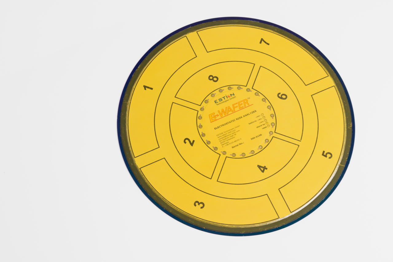
The E-Wafer embeds measuring devices for electrostatic charges within a 200mm or 300mm wafer, which allows in-situ measurements from within the production process.
Wafers are affected by electrostatic charges in several different ways. Firstly there are the damages caused by electrostatic discharges on the wafer, which develop to be a bigger problem the smaller the structures of the circuits get. In addition to this, electrostatic charges cause the accumulation of particles on the wafer-surface leading to defects. Wet processes can also cause electric charges and non-uniformity in the films on the wafer surface.
All three of these causes for electrostatic damage on the wafer surface can be analyzed precisely with the E-Wafer. It provides in-situ measurements throughout the entire production process, analyzing the potential differences within the wafer-surface on eight areas related to the middle. Equipped with an integrated real-time clock, memory, and WLAN connection and supplemented by the supplied analyzing software, this provides all the necessary data to analyze and pinpoint critical points where electrostatic problems can occur. By implementing counter measures at these points, the number of rejects leaving the production process can be reduced significantly.
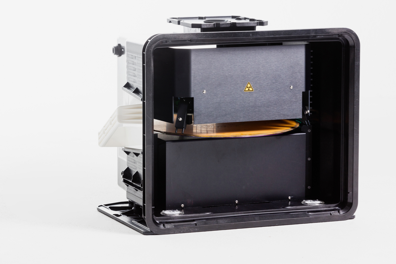
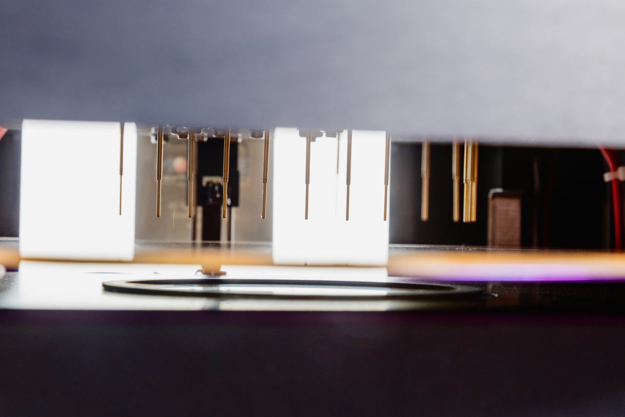
The E-Wafer is designed for the continuous and automated control of the production process. The 300mm variation docking station is built into a ShinEtsu FOUP to integrate it seamlessly into the automated production process. The 200mm variation comes in an open or a SMIF-compatible cassette – again for easy integration. Both variants are also available with portable docking stations for use as a risk analyzer in R&D.
Contact us for further information! We are happy to make up an individual quote for you.